
Onsemi MMUN2230LT1G: A Comprehensive Technical Overview of the NPN Digital Transistor
The Onsemi MMUN2230LT1G represents a highly integrated solution within the realm of surface-mount discrete semiconductors. This component is not a simple transistor but a monolithic digital transistor, a building block engineered to streamline circuit design and reduce component count on PCBs. It incorporates a single NPN bipolar junction transistor (BJT) with a fully integrated bias resistor network, making it an ideal choice for interface, driver, and switching applications in a vast array of consumer and industrial electronics.
Internal Architecture and Key Features
At its core, the MMUN2230LT1G is an NPN digital transistor. The "digital" designation signifies its built-in resistor network. Specifically, it features a 10 kΩ base resistor (R1) and a 10 kΩ pull-down resistor (R2) connected between the base and emitter. This integration is the device's most significant advantage. The inclusion of R2 ensures the transistor is firmly held in the 'OFF' state in the absence of an input signal, providing excellent noise immunity and preventing false triggering. The base resistor (R1) simplifies direct interfacing with microcontrollers (MCUs) or other logic circuits, as it limits the base current, eliminating the need for an external current-limiting resistor.
Housed in a compact, industry-standard SOT-23-3 package, this transistor is designed for high-density board layouts. Its small footprint is critical for modern, miniaturized electronic devices. The device is characterized by its ability to switch loads efficiently, with a continuous collector current (Ic) rating of 100 mA and a collector-emitter voltage (Vceo) of 50 V. This robust voltage and current handling capability allows it to drive a variety of loads, including relays, LEDs, solenoids, and motors, directly from the output pins of a logic IC or microcontroller.
Electrical Characteristics and Performance
The electrical parameters of the MMUN2230LT1G are tailored for reliable digital switching. The saturation region, where the transistor behaves as a closed switch, is a key area of operation. The device exhibits a low collector-emitter saturation voltage (Vce(sat)), typically around 0.25V at Ic=10mA and Ib=0.5mA. A low Vce(sat) minimizes power loss and heat generation when the transistor is fully 'ON,' enhancing overall efficiency.
Furthermore, its DC current gain (hFE) is specified under conditions that include the internal resistors, providing designers with a clear understanding of the input current required to achieve the desired output current. The integrated resistors ensure consistent performance and reduce the parametric variations that can occur when using discrete resistors.
Application Circuits and Usage
The primary application for the MMUN2230LT1G is as an inverter or a buffer. A typical inverter circuit involves connecting the input signal directly to the device's input pin (which connects internally to R1). The output is taken from the collector, with a load resistor connected to a positive supply rail. When the input is logic 'HIGH', the transistor turns on, pulling the output (collector) to near ground potential (logic 'LOW'). Conversely, a logic 'LOW' input turns the transistor off, allowing the output to be pulled up to the supply rail (logic 'HIGH').
It is also extensively used for driving inductive loads like small DC relays. A flyback diode is recommended to be used in parallel with the inductive load to suppress voltage spikes generated when the current is suddenly interrupted during turn-off, thereby protecting the transistor from potential damage.
Advantages and Design Considerations
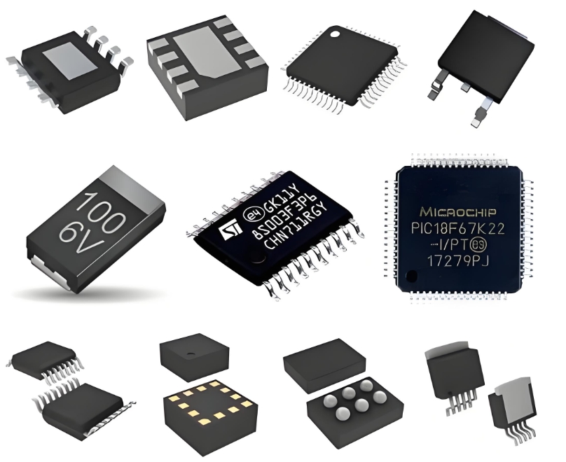
The major advantages of using the MMUN2230LT1G are:
Board Space Savings: Integrates two resistors, reducing part count and PCB area.
Simplified Assembly: Fewer components lower manufacturing costs and improve reliability.
Design Simplification: Eases the circuit design process and bill of materials (BOM) management.
Improved Noise Immunity: The internal pull-down resistor ensures a stable off-state.
Designers must consider that the internal resistors are fixed and cannot be customized for specific applications. The input threshold voltage is determined by the internal R1 and the required base current. Therefore, ensuring the driving source can provide sufficient voltage and current to overcome the R1 value and saturate the transistor is crucial for proper operation.
ICGOODFIND: The Onsemi MMUN2230LT1G is a quintessential example of how integration can optimize electronic design. It delivers robust performance, enhanced reliability, and significant space savings, making it an superior alternative to discrete NPN transistors and resistor combinations. Its role as an efficient interface between low-power control logic and higher-power loads solidifies its position as a fundamental component in countless modern digital circuits.
Keywords:
1. NPN Digital Transistor
2. Integrated Resistor Network
3. SOT-23-3 Package
4. Saturation Voltage (Vce(sat))
5. Logic Interface / Switching

